
In recent years, the LCC resonant converter has attracted much attention because it is superior to conventional series resonant converters and parallel resonant converters: when the load and input change greatly, the frequency change is still small, and switching in the full load range can achieve zero voltage conversion (ZVS). What is the design process of LLC resonant circuit?
Madison 게시 날짜 July 31, 2020
For the series resonant converter (SRC), the rectifier load network is connected in series with an LC resonant network, as shown in Figure 1. From this structure, the resonant network and the load act as a voltage divider. By changing the frequency of the driving voltage Vd, the impedance of the resonant network is changed. The input voltage will be distributed to this part of the impedance and reflected load. Because it is a voltage divider, the SRC DC gain is always less than 1. Under small load conditions, the load impedance is very large relative to the impedance of the resonant network; all input voltage falls on the load. This makes it difficult to adjust the output under light load conditions. Theoretically, when the output is adjusted under no load, the frequency will become infinite.
For a parallel resonant converter, the rectifier load network and the resonant capacitor are connected in parallel, as shown in the figure. Since the load is connected in parallel with the resonant network, there is inevitably a large amount of circulating current. This makes it difficult for people to use parallel resonant circuits in high-power situations.


In order to solve the limitations of traditional resonant converters, LLC resonant converters are proposed. Compared with conventional resonators, LLC-type resonant converters have many advantages. First of all, it can adjust the output under a wide range of input and load changes, while the switching frequency changes relatively little. Second, it can achieve zero voltage switching (ZVS) in the entire operating range. Finally, all parasitic elements, including the junction capacitance of all semiconductor devices and the leakage inductance and magnetizing inductance of the transformer, are used to achieve ZVS.
Anthony 게시 날짜 July 31, 2020
Design Flow
Use the schematic diagram in Figure 10 as a reference to describe the design process. A DC/DC converter with an output of 125W/24V is selected as a design example. The design specifications are as follows:
-Input voltage: 380Vdc (PFC level output)
-Output: 24V/5A (120W)
-Hold time requirement: 17ms
-DC link capacitance of PFC output terminal: 100uf

Step 1] Define system parameters
The first step must define the following parameters.
Estimated efficiency (Eff): The estimated power conversion efficiency is mainly used to calculate the maximum input power at a certain maximum output power. If there is no available reference value, for low-voltage output applications, Eff generally takes 0.88~0.92; for high-voltage output applications, Eff generally takes 0.92~0.96. With the estimated efficiency, the highest input power can be calculated.

-Input voltage range (Vinmin and Vinmax): Normally, it is assumed that the input voltage is provided by the output of the power factor correction (PFC) pre-regulator. When the PFC output provides the input voltage, considering the hold time requirement, the minimum input voltage is.
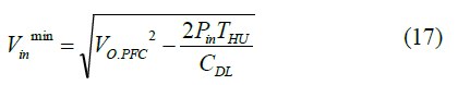
Among them, VO.PFC is the rated output voltage of the PFC, THU is the hold time, and CDL is the DC link (DC link) large capacitor.
The maximum input voltage is:
