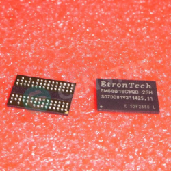
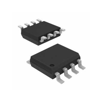
DDR2 32Mx16 PC800


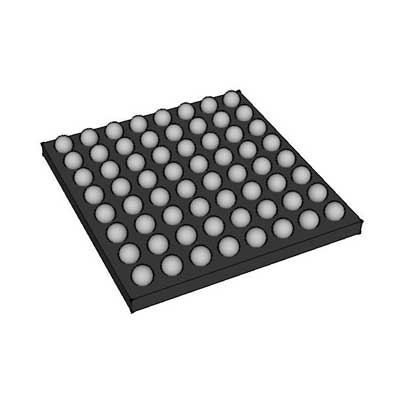
이미지는 참고용입니다..
제품 세부정보는 제품 사양을 참조하세요.
DDR2 32Mx16 PC800
$200 이상 주문 시 한정판 중국 스타일 선물을 받으실 수 있습니다..
1000달러 이상 주문 시 배송비 30달러가 면제됩니다..
$5000 이상 주문 시 배송비 및 거래 수수료가 면제됩니다..
이 혜택은 신규 고객과 기존 고객 모두에게 적용되며 2024년 1월 1일부터 2024년 12월 31일까지 유효합니다..
Etron
EM68B16CWQH-25H datasheet
FBGA-84
기억
지금 견적 요청을 제출하시면 1년 이내에 견적을 제공해 드릴 예정입니다. 4월 19, 2024. 지금 주문하시면 이내에 거래가 완료될 것으로 예상됩니다. 4월 24, 2024. Ps:시간은 GMT+8:00 기준입니다.


• JEDEC Standard Compliant
• JEDEC standard 1.8V I/O (SSTL_18-compatible)
• Power supplies: VDD & VDDQ = +1.8V ± 0.1V
• Operating temperature: TC = 0~85°C
• Supports JEDEC clock jitter specification
• Fully synchronous operation
• Fast clock rate: 333/400/533MHz
• Differential Clock, CK & CK#
• Bidirectional single/differential data strobe
- DQS & DQS#
• 4 internal banks for concurrent operation
• 4-bit prefetch architecture
• Internal pipeline architecture
• Precharge & active power down
• Programmable Mode & Extended Mode registers
• Posted CAS# additive latency (AL): 0, 1, 2, 3, 4, 5, 6
• WRITE latency = READ latency - 1 tCK
• Burst lengths: 4 or 8
• Burst type: Sequential / Interleave
• DLL enable/disable
• Off-Chip Driver (OCD)
- Impedance Adjustment
- Adjustable data-output drive strength
• On-die termination (ODT)
• RoHS compliant
• Auto Refresh and Self Refresh
• 8192 refresh cycles / 64ms
• 84-ball 8x12.5x1.2mm (max) FBGA
- Pb and Halogen Free
Description:
Overview The EM68B16C is a high-speed CMOS DoubleData-Rate-Two (DDR2), synchronous dynamic randomaccess memory (SDRAM) containing 512 Mbits in a 16- bit wide data I/Os. It is internally configured as a quad bank DRAM, 4 banks x 8Mb addresses x 16 I/Os. The device is designed to comply with DDR2 DRAM key features such as posted CAS# with additive latency, Write latency = Read latency -1, Off-Chip Driver (OCD) impedance adjustment, and On Die Termination(ODT). All of the control and address inputs are synchronized with a pair of externally supplied differential clocks. Inputs are latched at the cross point of differential clocks (CK rising and CK# falling). All I/Os are synchronized with a pair of bidirectional strobes (DQS and DQS#) in a source synchronous fashion. The address bus is used to convey row, column, and bank address information in RAS #, CAS# multiplexing style. Accesses begin with the registration of a Bank Activate command, and then it is followed by a Read or Write command. Read and write accesses to the DDR2 SDRAM are 4 or 8-bit burst oriented; accesses start at a selected location and continue for a programmed number of locations in a programmed sequence. Operating the four memory banks in an interleaved fashion allows random access operation to occur at a higher rate than is possible with standard DRAMs. An auto precharge function may be enabled to provide a self-timed row precharge that is initiated at the end of the burst sequence. A sequential and gapless data rate is possible depending on burst length, CAS latency, and speed grade of the device.

WQ: indicates 8x12.5x1.2mm (max) FBGA package
H: indicates Generation Code
H*: indicates Pb and Halogen Free

Request a quote EM68B16CWQH-25H at censtry.com. All items are new and original with 365 days warranty! The excellent quality
and guaranteed services of EM68B16CWQH-25H in stock for sale, check stock quantity and pricing,
view product specifications, and order contact us:sales@censtry.com.
The price and lead time for EM68B16CWQH-25H depending on the quantity required, please send your request to us,
our sales team will provide you price and delivery within 24 hours, we sincerely look forward to cooperating with you.

TI
611 PCS
TIL311 .PDF
TOSHIBA
1000 PCS
THGBM5G8A4JBAIR .PDF
TOSHIBA
5822 PCS
TD62784APG .PDF
MICROCHIP
16500 PCS
TCN75AVOA713 .PDF
2024-04-18
Great Partner
2024-04-18
Great service, quick response!
2024-04-18
Jim is a pleasure to work with.
2024-04-18
HELPFUL and NICE people
2024-04-17
I have bought from Censtry for over 10 years and they are a trusted and terrific supplier. Their parts have always passed our inspection, and we like all the people we deal with at Censtry: Marc, Linda, Andrea and John. They get an A+ in customer service.
2024-04-16
If they show an item speak with Jayson he will help you out. Thanks
2024-04-13
Jackie is a true professional, and runs a great, professional company. A true Leader in our industry. Very flexible, and fair; We will look for future opportunities to do business with Maverick again!
2024-04-08
Just did a large order with Censtry in China and they were excellent. Very good supplier.
2024-03-28
Kevin is a solid guy..Never a problem!
2024-03-07
Lisa is a pleaseure to deal with
우리는 귀하의 피드백을 매우 소중하게 생각합니다. 가장 솔직한 리뷰를 공유해주세요.
*코멘트를 게시하기 전에 계정에 로그인하세요