7월 14, 2023
2820
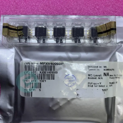
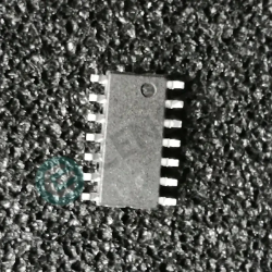
The TDA2822M is a monolithic integrated circuit designed for audio applications. It comes in an 8-lead Minidip package, making it suitable for compact electronic devices such as portable cassette players and radios. The main purpose of the TDA2822M is to serve as a dual audio power amplifier, delivering amplified audio signals to the speakers or headphones. Its dual-channel configuration, low voltage operation, decent power output, and low distortion characteristics make it a popular choice for many audio applications.
TDA2822M Equivalent or Replacement
TDA2822M Audio Amplifier Circuit
More Information: https://www.censtry.com/product/st/tda2822m-.html
https://www.st.com/resource/en/datasheet/cd00000134.pdf

KA2209
S1A2209A01-D0B0
LM386
TDA2822
PAM8403
MC34119
This basic circuit demonstrates a single-ended configuration for one channel of the TDA2822M IC. To implement stereo audio amplification, a similar circuit can be replicated for the second channel using the remaining pins (OUT2, IN2, and GND). It is essential to consult the datasheet of the TDA2822M IC for additional information on recommended component values, input impedance, output power, and any additional circuitry requirements for optimal performance.
Power Supply: The circuit is powered by a +12V supply voltage connected to the VCC pin (Pin 8) of the TDA2822M IC. The GND pin (Pin 4) is connected to the ground (GND) reference of the circuit.
Input Signals: The audio input signals are connected to IN1 (Pin 7) and IN2 (Pin 5) of the IC. These input pins are usually connected to a source such as an audio player or a microphone.
Coupling Capacitor: Capacitor C1 (10μF) is used for DC blocking and coupling purposes. It is connected between the audio input source and the input pins IN1 and IN2 of the IC.
Output Connections: The amplified audio output signals are obtained from OUT1 (Pin 1) and OUT2 (Pin 3) of the IC. These pins are connected to the positive terminals of the speakers or headphones.
Ground Connection: The GND pin (Pin 4) of the IC is connected to the ground reference of the circuit. It provides a common ground connection for both the amplifier and the audio source.
Basic Circuit Diagram for An Audio Amplifier Using the TDA2822M IC

The TDA2822M IC has a wide range of acceptable input voltage levels. The recommended input voltage for the TDA2822M is typically between 0.3V and VCC (supply voltage). It is important to note that the input voltage should not exceed the supply voltage (VCC) specified for the IC. Consulting TDA2822M datasheet is highly recommended for input voltage specifications.
To achieve the best performance and avoid distortion, it is advisable to ensure that the input voltage is within the specified range and matches the desired operating conditions. Additionally, it is important to consider the input impedance of the TDA2822M, which is typically around 30 kΩ.
Dual-channel configuration
Low voltage operation
High power output
Low distortion and noise
Wide frequency response
Simple external circuitry
Thermal protection
Minidip package
Portable Audio Players
Personal Stereos
TV and Multimedia Systems
Intercom Systems
Instrument Amplification
Voice Communication Devices
Educational and DIY Projects

Reference: https://www.st.com/resource/en/datasheet/cd00000134.pdf
TDA2822M Symbol
TDA2822M Footprint
TDA2822M 3D Model