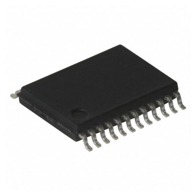
IC PWR SWITCH N-CHAN 1:1 SOT23-6


이미지는 참고용입니다..
제품 세부정보는 제품 사양을 참조하세요.
IC PWR SWITCH N-CHAN 1:1 SOT23-6
$200 이상 주문 시 한정판 중국 스타일 선물을 받으실 수 있습니다..
1000달러 이상 주문 시 배송비 30달러가 면제됩니다..
$5000 이상 주문 시 배송비 및 거래 수수료가 면제됩니다..
이 혜택은 신규 고객과 기존 고객 모두에게 적용되며 2024년 1월 1일부터 2024년 12월 31일까지 유효합니다..
TI
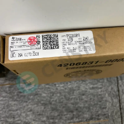
TPS22810DBVR datasheet
SOT-23-6
IC 칩
 Lead free/RoHS Compliant
지금 견적 요청을 제출하시면 1년 이내에 견적을 제공해 드릴 예정입니다. 5월 02, 2024. 지금 주문하시면 이내에 거래가 완료될 것으로 예상됩니다. 5월 07, 2024. Ps:시간은 GMT+8:00 기준입니다.


1 Features
• Integrated Single Channel Load Switch
• Ambient Operating Temperature:
–40°C to +105°C
– SOT23-6 (DBV): 2-A Maximum Continuous Current 1
– WSON (DRV): 3-A Maximum Continuous Current 1
• Input Voltage Range: 2.7 V to 18 V
• Absolute Maximum Input Voltage: 20 V
• On-Resistance (RON)
– RON = 79 mΩ (typical) at VIN = 12 V
• Quiescent Current
– 62 µA (typical) at VIN = 12 V
• Shutdown Current
– 500 nA (typical) at VIN = 12 V
• Thermal Shutdown
• Undervoltage Lock-Out (UVLO)
• Adjustable Quick Output Discharge (QOD)
• Configurable Rise Time With CT Pin
• SOT23-6 Package
– 2.9-mm × 2.8-mm, 0.95-mm Pitch
1.45-mm Height (DBV)
• WSON Package
– 2-mm × 2-mm, 0.65-mm Pitch 0.75-mm Height (DRV)
• ESD Performance Tested per JESD 22
– ±2-kV HBM and ±1-kV CDM
(1) Thermal performance must be considered
2 Applications
• HD TV
• Industrial Systems
• Set Top Box
• Surveillance systems
3 Description
The TPS22810 is a single channel load switch with configurable rise time and with an integrated quick output discharge (QOD). In addition, the device features thermal shutdown to protect the device against high junction temperature. Because of this, safe operating area of the device is inherently ensured. The device contains an N-channel MOSFET that can operate over an input voltage range of 2.7 V to 18 V. SOT23-5 (DBV) package can support a maximum current of 2 A. WSON (DRV) package can support a maximum current of 3 A. The switch is controlled by an on and off input, which is capable of interfacing directly with low-voltage control signals.
The configurable rise time of the device greatly reduces inrush current caused by large bulk load capacitances, thereby reducing or eliminating power supply droop. Undervoltage lock-out is used to turn off the device if the VIN voltage drops below a threshold value, ensuring that the downstream circuitry is not damaged by being supplied by a voltage lower than intended. The configurable QOD pin controls the fall time of the device to allow design flexibility for power down.
The TPS22810 is available in a leaded, SOT-23 package (DBV) which allows to visually inspect solder joints, as well as a WSON package (DRV). The device is characterized for operation over the free-air temperature range of –40˚C to +105˚C.

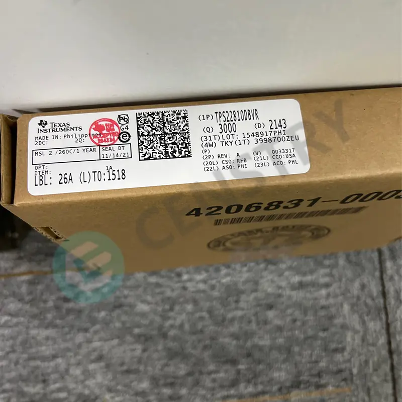
Request a quote TPS22810DBVR at censtry.com. All items are new and original with 365 days warranty! The excellent quality
and guaranteed services of TPS22810DBVR in stock for sale, check stock quantity and pricing,
view product specifications, and order contact us:sales@censtry.com.
The price and lead time for TPS22810DBVR depending on the quantity required, please send your request to us,
our sales team will provide you price and delivery within 24 hours, we sincerely look forward to cooperating with you.
TI
2718 PCS
TISP61511DR .PDF
TI
886 PCS
TISP61089HDMR .PDF
TI
4602 PCS
TISP61089BDR .PDF
TI
47 PCS
TISP61089BD .PDF
2024-05-01
Excellent fast postage
2024-05-01
Ware dankend erhalten!
2024-05-01
Tested ALL OK!!!
2024-05-01
Excellent ***** Highly recommended - Thank you.
2024-04-30
Worked like a charm... thanks
2024-04-28
Llegó bien
2024-04-24
Would use Iceberg again. Good response to enquiry and requests.
2024-04-16
Great! recommended !
2024-03-31
We are very pleased with our business with her, and look to give her every PO we can. Thanks Dusty.
2024-02-28
Very reliable and delivered as promised. Mark and Wendy, great job! Thanks again.

우리는 귀하의 피드백을 매우 소중하게 생각합니다. 가장 솔직한 리뷰를 공유해주세요.
*코멘트를 게시하기 전에 계정에 로그인하세요