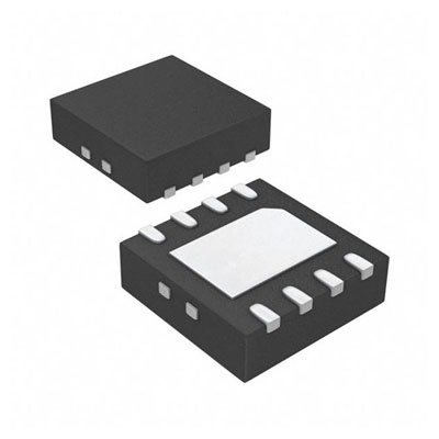
IC PWR SWITCH N-CHAN 1:1 8WSON


이미지는 참고용입니다..
제품 세부정보는 제품 사양을 참조하세요.
IC PWR SWITCH N-CHAN 1:1 8WSON
$200 이상 주문 시 한정판 중국 스타일 선물을 받으실 수 있습니다..
1000달러 이상 주문 시 배송비 30달러가 면제됩니다..
$5000 이상 주문 시 배송비 및 거래 수수료가 면제됩니다..
이 혜택은 신규 고객과 기존 고객 모두에게 적용되며 2024년 1월 1일부터 2024년 12월 31일까지 유효합니다..
TI
TPS22962DNYR datasheet
WSON-8
IC 칩
 Lead free/RoHS Compliant
지금 견적 요청을 제출하시면 1년 이내에 견적을 제공해 드릴 예정입니다. 5월 02, 2024. 지금 주문하시면 이내에 거래가 완료될 것으로 예상됩니다. 5월 06, 2024. Ps:시간은 GMT+8:00 기준입니다.


1 Features
• Integrated Single Channel Load Switch
• VBIAS Voltage Range: 2.5 V to 5.5 V
• VIN Voltage Range: 0.8 V to 5.5 V
• Ultra Low RON Resistance
– RON = 4.4 mΩ at VIN = 5 V (VBIAS = 5 V)
• 10 A Maximum Continuous Switch Current
• Low Quiescent Current
– (20 µA for VBIAS = 5 V)
• Low Shutdown Current
– (1 µA for VBIAS = 5 V)
• Low Control Input Threshold Enables Use of 1.2 V or Higher GPIO
• Controlled and Fixed Slew Rate Across VBIAS and VIN
– tR = 2663 µs at VIN = 5 V (VBIAS = 5 V)
• Quick Output Discharge (QOD)
• SON 8-Pin Package with Thermal Pad
• ESD Performance Tested per JESD 22
– 2-kV Human-Body Model (HBM)
– 1-kV Charged-Device Model (CDM)
2 Applications
• Servers
• Medical
• Telecom Systems
• Computing
• Industrial Systems
• High Current Voltage Rails
3 Description
The TPS22962 is a small, ultra-low RON, single channel load switch with controlled turn on. The device contains an N-channel MOSFET that can operate over an input voltage range of 0.8 V to 5.5 V and supports a maximum continuous current of 10 A.
The combination of ultra-low RON and high current capability of the device makes it ideal for driving processor rails with very tight voltage dropout tolerances. The controlled rise time of the device greatly reduces inrush current caused by large bulk load capacitances, thereby reducing or eliminating voltage droop on the power supply. The switch can be independently controlled via the ON pin, which is capable of interfacing directly with low-voltage control signals originating from microcontrollers or low voltage discrete logic. The device further reduces the total solution size by integrating a 224-Ω pull-down resistor for quick output discharge (QOD) when the switch is turned off.
The TPS22962 is available in a small 3.00 mm x 3.00 mm WSON-8 package (DNY). The DNY package integrates a thermal pad which allows for high power dissipation in high current and high temperature applications. The device is characterized for operation over the free-air temperature range of –40°C to 105°C.

Request a quote TPS22962DNYR at censtry.com. All items are new and original with 365 days warranty! The excellent quality
and guaranteed services of TPS22962DNYR in stock for sale, check stock quantity and pricing,
view product specifications, and order contact us:sales@censtry.com.
The price and lead time for TPS22962DNYR depending on the quantity required, please send your request to us,
our sales team will provide you price and delivery within 24 hours, we sincerely look forward to cooperating with you.
TI
2718 PCS
TISP61511DR .PDF
TI
886 PCS
TISP61089HDMR .PDF
TI
4602 PCS
TISP61089BDR .PDF
TI
47 PCS
TISP61089BD .PDF
2024-05-01
worked fine thanks
2024-04-30
Fast delivery, good quality
2024-04-30
todo en perfectas condiciones gracias.
2024-04-29
Works perfect.Thanks
2024-04-27
Todo bien mas que contento. Gracias
2024-04-24
llego rápido y todo lo que pedí, de buena calidad.

우리는 귀하의 피드백을 매우 소중하게 생각합니다. 가장 솔직한 리뷰를 공유해주세요.
*코멘트를 게시하기 전에 계정에 로그인하세요