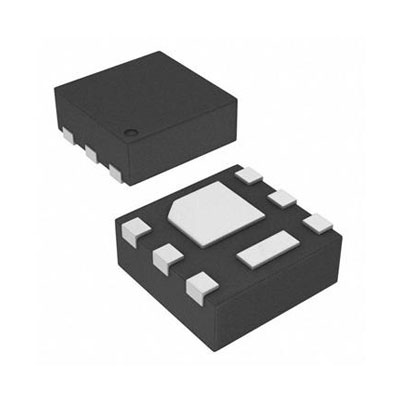
IC REG BOOST PROG 0.7A SYNC 6SON


이미지는 참고용입니다..
제품 세부정보는 제품 사양을 참조하세요.
IC REG BOOST PROG 0.7A SYNC 6SON
$200 이상 주문 시 한정판 중국 스타일 선물을 받으실 수 있습니다..
1000달러 이상 주문 시 배송비 30달러가 면제됩니다..
$5000 이상 주문 시 배송비 및 거래 수수료가 면제됩니다..
이 혜택은 신규 고객과 기존 고객 모두에게 적용되며 2024년 1월 1일부터 2024년 12월 31일까지 유효합니다..
TI
TPS61291DRVR datasheet
WSON-6
전원 관리 IC
 Lead free/RoHS Compliant
지금 견적 요청을 제출하시면 1년 이내에 견적을 제공해 드릴 예정입니다. 7월 28, 2024. 지금 주문하시면 이내에 거래가 완료될 것으로 예상됩니다. 7월 31, 2024. Ps:시간은 GMT+8:00 기준입니다.


1 Features
• Input Voltage Range 0.9V to 5V
• Startup Voltage 1.5V at 20mA Load
• Pin Selectable Output Voltages: 3.3V, 3V, 2.5V
• 15nA typical Quiescent Current in Bypass Mode
• 5.7μA typical Quiescent Current in Boost Mode
• Bypass Switch from VIN to VOUT
• IOUT > 200mA at 3.3V VOUT, VIN = 1.8V
• Internal Feedback Divider Disconnect (Bypass Mode)
• Controlled Bypass Transition Prevents Reverse Current into Battery
• Power-Save Mode at Light Loads
• Overtemperature Protection
• Redundant Overvoltage Protection
• Small 2mm x 2mm SON 6-pin package
2 Applications
• Metering (Gas, Water, Smart Meters)
• Remote Controls
• Home Security / Home Automation
• Single 3V Li-MnO2 or 2 x 1.5V Alkaline Cell Powered Applications
3 Description
The TPS61291 is a boost converter with pin selectable output voltages and an integrated bypass mode. In bypass operation, the device provides a direct path from the input to the system and allows a low power micro controller (MCU) such as the MSP430 to operate directly from a single 3V Li-MnO2 battery or dual alkaline battery cells.
In bypass mode the integrated feedback divider network for boost mode operation is disconnected from the output and the quiescent current consumption drops down to only 15nA (typical).
In boost mode the device provides a minimum output current of 200mA at 3.3V VOUT from 1.8V VIN. The boost mode is used for system components which require a regulated supply voltage and cannot directly operate from the input source. The boost converter is based on a current-mode controller using synchronous rectification to obtain maximum efficiency and consumes typically 5.7uA from the output. During startup of the boost converter, theVSEL pin is read out and the integrated feedback network sets the output voltage to 2.5V, 3V or 3.3V.
Bypass mode or boost mode operation is controlled by the system via the EN/BYP pin. The device integrates an enhanced bypass mode
control to prevent charge, stored in the output capacitor during boost mode operation, from flowing back to the input and charging the battery.
The device is packaged in a small 6-pin SON package (DRV) measuring 2.0mm × 2.0mm x 0.75mm.


Request a quote TPS61291DRVR at censtry.com. All items are new and original with 365 days warranty! The excellent quality
and guaranteed services of TPS61291DRVR in stock for sale, check stock quantity and pricing,
view product specifications, and order contact us:sales@censtry.com.
The price and lead time for TPS61291DRVR depending on the quantity required, please send your request to us,
our sales team will provide you price and delivery within 24 hours, we sincerely look forward to cooperating with you.
TI
8000 PCS
LMD18201T .PDF
TI
4470 PCS
INA240A3PWR .PDF
TI
62900 PCS
TPS7B8250QDRVRQ1 .PDF
TI
380948 PCS
TPS7B8150QDRVRQ1 .PDF
2024-07-26
Great ! Like always !
2024-07-26
We like, thank you
2024-07-26
Great value, as description, thanks :-)

우리는 귀하의 피드백을 매우 소중하게 생각합니다. 가장 솔직한 리뷰를 공유해주세요.
*코멘트를 게시하기 전에 계정에 로그인하세요