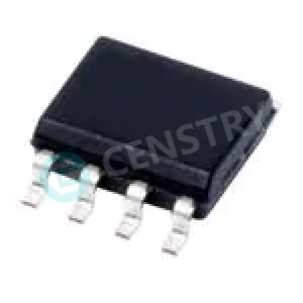
Translation - Voltage Levels 8B Bidir Voltage- Level Translator


이미지는 참고용입니다..
제품 세부정보는 제품 사양을 참조하세요.
Translation - Voltage Levels 8B Bidir Voltage- Level Translator
$200 이상 주문 시 한정판 중국 스타일 선물을 받으실 수 있습니다..
1000달러 이상 주문 시 배송비 30달러가 면제됩니다..
$5000 이상 주문 시 배송비 및 거래 수수료가 면제됩니다..
이 혜택은 신규 고객과 기존 고객 모두에게 적용되며 2024년 1월 1일부터 2024년 12월 31일까지 유효합니다..
TI
TXB0106PWR datasheet
TSSOP16
논리 IC
 Lead free/RoHS Compliant
지금 견적 요청을 제출하시면 1년 이내에 견적을 제공해 드릴 예정입니다. 5월 17, 2024. 지금 주문하시면 이내에 거래가 완료될 것으로 예상됩니다. 5월 22, 2024. Ps:시간은 GMT+8:00 기준입니다.


Features
● 1.2Vto3.6VonAPortand1.65to5.5Von B Port (VccA≤Vcce)
● Vcc Isolation Feature - If Either Vcc Input Is at GND, All Outputs Are in the High-lmpedance State
● OE Input Circuit Referenced to VccA
● Low-Power Consumption, 4 μA Max lcc lof Supports Partial-Power-Down Mode Operation
● Latch-Up Performance Exceeds 100 mA Per JESD 78, Class II
● ESD Protection Exceeds JESD 22
● APort.
● 2500 V Human Body Model (A114-B)
● 150 V Machine Model (A115-A)
● 1500 V Charged-Device Model (C101)
● B Port
● +15 kV Human Body Model (A114-B)
● 150 V Machine Model (A115-A)
● 1500 V Charged-Device Model (C101)
Applications
● Headset
● Smartphone
● Tablet
● Desktop PC
Description
This 6-bit noninverting translator uses two separate configurable power-supply rails. The A port is designed to track VCCA. Vccz accepts any supply voltage from 1.2 V to 3.6 V. The B port is designed to track Vcce. VccB accepts any supply voltage from 1.65 V to 5.5 V. This allows for universal low-voltage bidirectional translation between any of the 1.2 V, 1.5 V, 1.8 V, 2.5 V, 3.3 V, and 5 V voltage nodes. VCcA should not exceed Vcce.
When the output-enable (OE) input is low, all outputs are placed in the high-impedance state.
The TXB0106 is designed so that the OE input circuit is supplied by VccA.
This device is fully specified for partial-power-down applications using lf The loff circuitry disables the outputs,preventing damaging current backflow through the device when it is powered down.
To ensure the high-impedance state during power up or power down, OE should be tied to GND through a pulldown resistor; the minimum value of the resistor is determined by the current sourcing capability of the driver.

Typical Application Block Diagram for TXB010X

Pin Configuration and Functions

Request a quote TXB0106PWR at censtry.com. All items are new and original with 365 days warranty! The excellent quality
and guaranteed services of TXB0106PWR in stock for sale, check stock quantity and pricing,
view product specifications, and order contact us:sales@censtry.com.
The price and lead time for TXB0106PWR depending on the quantity required, please send your request to us,
our sales team will provide you price and delivery within 24 hours, we sincerely look forward to cooperating with you.
TI
8000 PCS
LMD18201T .PDF
TI
12000 PCS
INA381A2IDSGR .PDF
TI
4470 PCS
INA240A3PWR .PDF
TI
62900 PCS
TPS7B8250QDRVRQ1 .PDF
2024-05-16
Great Company thank you
2024-05-16
Great company to deal with! They do what they promise!Always a pleasure to deal with Rosette.
2024-05-16
Great Company, Great Service
2024-05-16
Great supplier, thank you Eyal
2024-05-15
Great Service & Products
2024-05-15
Great vendor. Thanks for the service!!
2024-05-13
I will give a 5 star.
2024-05-11
I have had several transactions. Each went perfectly. They supplied us with some of the highest quality parts we have purchased in quite a long time. This company will earn your trust.
2024-05-05
it was a pleasant first deal, thanks Rebecca.
2024-04-25
Joe was great to deal with, smooth transaction. Will use again.

우리는 귀하의 피드백을 매우 소중하게 생각합니다. 가장 솔직한 리뷰를 공유해주세요.
*코멘트를 게시하기 전에 계정에 로그인하세요